
Semi Conductor Collection
"Unleashing the Power of Semiconductors: Revolutionizing Technology and Energy" Solar panels in the sun: Harnessing sunlight to power our world


All Professionally Made to Order for Quick Shipping
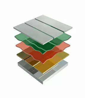
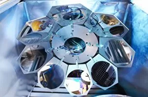
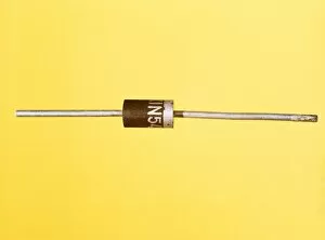
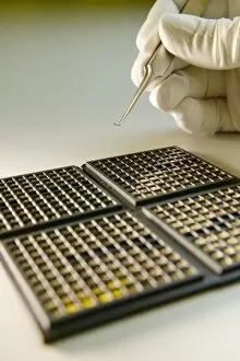
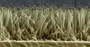
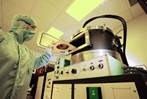
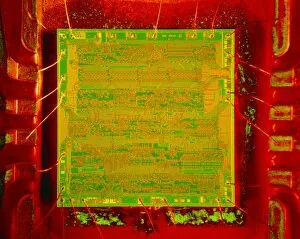
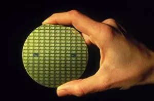
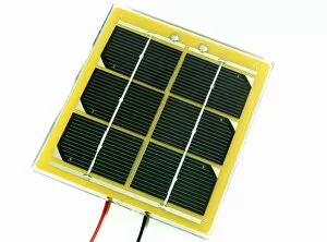
"Unleashing the Power of Semiconductors: Revolutionizing Technology and Energy" Solar panels in the sun: Harnessing sunlight to power our world, semiconductors pave the way for renewable energy solutions. Circuit board man: With every electronic device we use, semiconductors play a crucial role in enabling efficient communication and processing. Aerial view of Silicon Valley: The birthplace of innovation, this iconic image represents the heart of semiconductor technology development. Carbon nanotube computer model: Pushing boundaries with their extraordinary properties, carbon nanotubes hold immense potential for future computing systems. Domestic solar panel: Empowering homeowners to generate clean energy at their doorstep, semiconductors make residential solar panels possible. Circuit board components artwork F006 / 8627: An artistic representation showcasing the intricate beauty and complexity of circuitry made possible by semiconductors. Nanotube structure artwork C016 / 8888 & C016 / 8522: Celebrating the elegance and versatility of nanotubes as building blocks for advanced electronics and materials science. Organic light-emitting diode (OLED) artwork: Illuminating our lives with vibrant displays, OLEDs rely on semiconductors to emit light efficiently and create stunning visuals. MEMS production quality control: Ensuring precision manufacturing at microscale levels, semiconductor-based Micro-Electro-Mechanical Systems (MEMS) enhance various industries from healthcare to automotive engineering. Dark matter detector: Unveiling mysteries beyond our comprehension, cutting-edge detectors employ sophisticated semiconductor technologies in search of elusive dark matter particles. Gallium nitride nanowires SEM image: Exploring new frontiers in optoelectronics and high-power devices, gallium nitride nanowires exhibit exceptional performance due to their unique semiconductor properties.