Home > Science > SEM
Graphene transistor, SEM

![]()
Wall Art and Photo Gifts from Science Photo Library
Graphene transistor, SEM
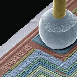
Graphene transistor. Coloured scanning electron micrograph (SEM) of a transistor composed of a graphene wire (centre), gold electrodes (dark yellow) and silicon (blue). The graphene wire is 200 nanometres (billionths of a metre) wide. Graphene is composed of a single layer of carbon atoms arranged in a honeycomb crystal lattice. It is both flexible and very strong. It conducts electrons faster than silicon and could one day replace silicon in applications such as nanometre (billionths of a metre) sized electronics, cheap and efficient solar panels, transparent window coatings and miniature sensing technologies. Graphene was discovered by Andre Geim in 2004
Science Photo Library features Science and Medical images including photos and illustrations
Media ID 6313773
© ANDRE GEIM, KOSTYA NOVOSELOV/SCIENCE PHOTO LIBRARY
Carbon Colored Conducting Conductor Contact Crystal Electrical Electrical Engineering Electrode Electrodes Electronics Gold Graphene Graphite Honey Comb Honey Combed Lattice Microscope Nanoelectronics Semi Conductor Sheet Silicon Switch Transistor Transmission Electron Transmission Electron Micrograph Wire Molecular Physical
EDITORS COMMENTS
This print showcases a graphene transistor, a groundbreaking technological marvel that holds immense potential for the future. In this colored scanning electron micrograph (SEM), we witness the intricate composition of this transistor. At its core lies a slender graphene wire, only 200 nanometers wide, surrounded by gold electrodes in dark yellow and silicon in blue. Graphene, an extraordinary material consisting of a single layer of carbon atoms arranged in a honeycomb crystal lattice, possesses remarkable properties. It boasts both flexibility and incredible strength while exhibiting superior electron conductivity compared to silicon. This exceptional characteristic positions graphene as a promising candidate to replace silicon in various applications such as nanometer-sized electronics. The discovery of graphene by Andre Geim in 2004 opened up new possibilities for scientific exploration and technological advancements. Its potential applications extend far beyond traditional electronics; it could revolutionize solar panels by enabling cost-effective and efficient solutions. Additionally, transparent window coatings and miniature sensing technologies may benefit from the unique attributes of this wonder material. In this image captured with precision using advanced microscopy techniques, we are granted a glimpse into the microscopic world where science meets innovation. The intricate network formed by the honeycombed lattice structure is truly mesmerizing—a testament to human ingenuity at harnessing nature's building blocks for progress in electrical engineering and nanoelectronics.
MADE IN THE UK
Safe Shipping with 30 Day Money Back Guarantee
FREE PERSONALISATION*
We are proud to offer a range of customisation features including Personalised Captions, Color Filters and Picture Zoom Tools
SECURE PAYMENTS
We happily accept a wide range of payment options so you can pay for the things you need in the way that is most convenient for you
* Options may vary by product and licensing agreement. Zoomed Pictures can be adjusted in the Basket.