
Microsystems Collection
Microsystems, the epitome of precision and innovation in technology. From MEMS production to quality control, every step is meticulously executed for flawless results


All Professionally Made to Order for Quick Shipping
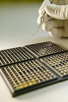
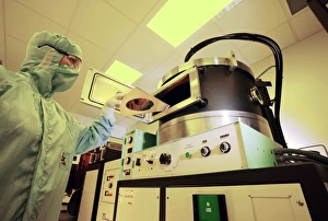
Microsystems, the epitome of precision and innovation in technology. From MEMS production to quality control, every step is meticulously executed for flawless results. In the realm of MEMS production, metal evaporation plays a crucial role. This process involves depositing thin layers of metal onto substrates with utmost accuracy, enabling the creation of intricate circuitry. Chemical etching further refines these microsystems by selectively removing material from silicon wafers. This technique allows for precise shaping and customization, ensuring optimal performance. External connections are vital in MEMS production as they facilitate seamless integration into larger systems. These connections enable efficient communication between microdevices and their surroundings, unlocking endless possibilities. Machined silicon wafers serve as the foundation for these microsystems. With their exceptional flatness and uniformity, they provide an ideal platform for various fabrication processes. Furnace processing takes center stage during MEMS production as it enables controlled heating and cooling cycles essential for achieving desired material properties. This meticulous treatment ensures durability and reliability. Quality control remains paramount throughout this intricate journey. Rigorous testing at each stage guarantees that only superior microsystems reach consumers' hands—ensuring satisfaction and trust in their functionality. Device sorting is another critical step where meticulous attention is given to categorizing products based on performance characteristics. This ensures that customers receive precisely tailored solutions to meet their specific needs. Support bonding brings together different components within a system seamlessly—a delicate dance requiring precision alignment and adhesion techniques to guarantee structural integrity. Thin film deposition adds yet another layer of sophistication to these marvels by coating them with ultra-thin films offering enhanced functionalities such as protection or sensing capabilities—an artistry achieved through advanced manufacturing techniques. Plasma etching contributes its magic by selectively removing materials using ionized gases—carving out intricate patterns with unparalleled precision while maintaining structural integrity—a testament to human ingenuity at its finest. Gold metal circuitry weaves its way through these microsystems, enabling efficient electrical conductivity and signal transmission.