
Acrylic Blox : Fabrication of integrated circuit wafers


![]()
Mounted Prints from Science Photo Library
Fabrication of integrated circuit wafers
Visual inspection of a photomask used in the fabrication of integrated circuit wafers at Seagate Microelectronics Ltd, Livingston, Scotland. The photomask is used in a photolithography process to selectively etch an electronic pattern onto a wafer of crystalline silicon - the base material for the ultimate integrated circuits that will be die stamped from the completed wafer
Science Photo Library features Science and Medical images including photos and illustrations
Media ID 6428963
© DAVID PARKER/SEAGATE MICROELECTRONICS LTD/ SCIENCE PHOTO LIBRARY
Chip Manufacture Electronic Electronics Integrated Circuit Micro Chip Semiconductor Industry Silicon Wafer Photolithography
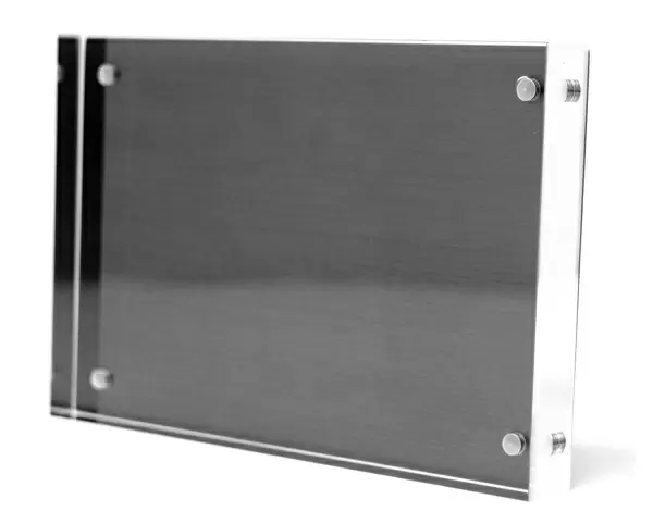
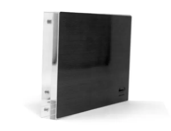
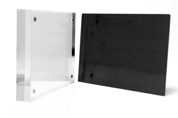
8"x6" (20x15cm) Acrylic Blox
Your photographic print is held in place by magnets and a micro thin sheet of metal covering the back of a 20mm piece of clear acrylic. Your print is held in place with magnets so can easily be replaced if needed.
Streamlined, one sided modern and attractive table top print
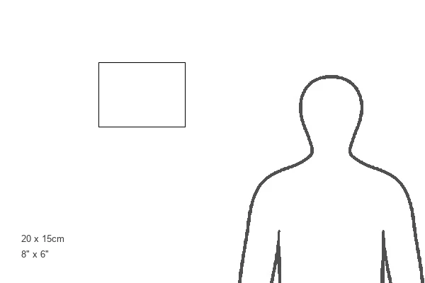
Estimated Product Size is 20.3cm x 15.2cm (8" x 6")
These are individually made so all sizes are approximate
Artwork printed orientated as per the preview above, with landscape (horizontal) orientation to match the source image.
EDITORS COMMENTS
This print showcases the intricate process of fabricating integrated circuit wafers at Seagate Microelectronics Ltd in Livingston, Scotland. The visual inspection captures a crucial step in chip manufacture - the examination of a photomask used during photolithography. In this highly advanced semiconductor industry, the photomask plays a pivotal role in selectively etching an electronic pattern onto a wafer made of crystalline silicon. This wafer serves as the foundation for creating cutting-edge integrated circuits that will eventually be die stamped from its completed form. The level of precision and attention to detail depicted in this image is truly awe-inspiring. Every element within this composition symbolizes innovation and technological advancement. From the delicate patterns on the photomask to the pristine surface of the silicon wafer, it is evident that every aspect has been meticulously crafted. As we delve into this mesmerizing world of electronics, it becomes clear how vital these processes are for our modern society. The seamless integration between science and technology showcased here highlights humanity's relentless pursuit of progress. Through photolithography and other groundbreaking techniques like those employed by Seagate Microelectronics Ltd, we witness firsthand how dreams become reality within these state-of-the-art facilities. This photograph encapsulates not only their expertise but also their commitment to pushing boundaries and shaping our future through microchip development.
MADE IN THE UK
Safe Shipping with 30 Day Money Back Guarantee
FREE PERSONALISATION*
We are proud to offer a range of customisation features including Personalised Captions, Color Filters and Picture Zoom Tools
SECURE PAYMENTS
We happily accept a wide range of payment options so you can pay for the things you need in the way that is most convenient for you
* Options may vary by product and licensing agreement. Zoomed Pictures can be adjusted in the Basket.